Effect of the Coatings on Planar Transmission Lines
Jan. 28, 2023
Takayuki HOSODA
Printed circuit boards are usually coated with solder resist to protect the copper foil,
and in some cases filler is also used,
but from a transmission line perspective, it is a factor that affects transmission line characteristics.
To understand the extent of this effect, we investigated the influence of resist and filler by 2D electromagnetic field analysis.
The result shows that even a resist twice as thick as the conductor's thickness of a typical FR4 board
can reduce a microstrip line with a characteristic impedance of 66 Ω to 62 Ω or less (≃ -7 %).
The effect is even greater in the case of conductor-backed coplanar transmission lines,
where a 56 Ω characteristic impedance can be reduced to as low as 49 Ω (≃ -12 %).
If filler as thick as the substrate is used, such as at BGA mounting points,
the reduction in characteristic impedance can be as much as -20%.
In the case of side-coupled lines,
the effect of resist on the characteristic impedance for even modes is small, at a few percent,
but for odd modes it can be as low as -10 %. in odd-numbered modes, it can be as much as -10 %,
so care must be taken when using it as a differential transmission line.
In terms of coupling, this means an increase in coupling of about 1 dB.
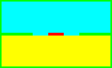
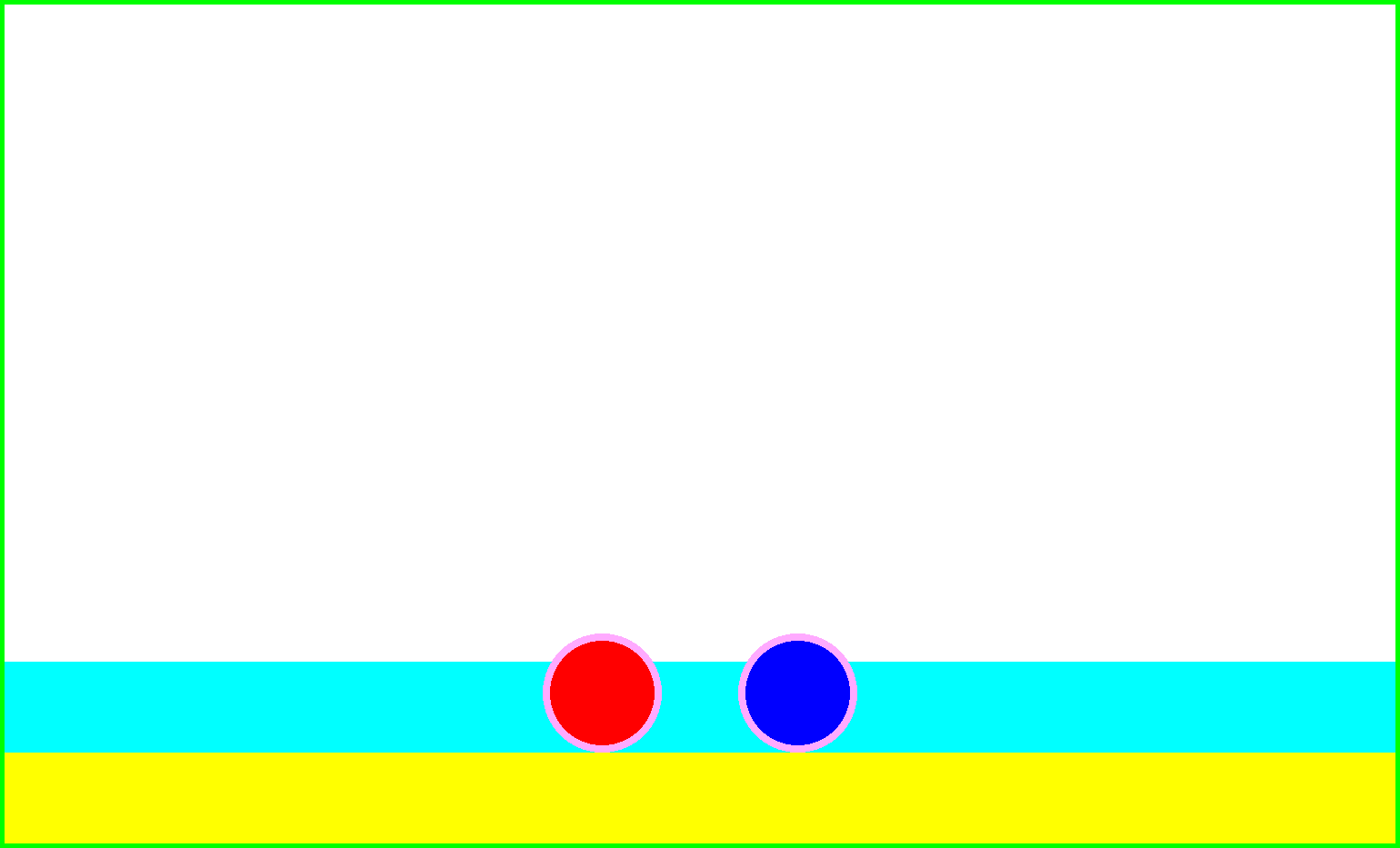
Color definitions of the transmission lines
█ Red     (#FF0000) : +Signal conductor
█ Blue    (#0000FF) : -Signal conductor
█ Green   (#00FF00) : Ground conductor
█ Yellow  (#FFFF00) : Substrate dielectric
█ Cyan    (#00FFFF) : Solder resist, filler or prepreg dielectric
█ Pink    (#FFAAFF) : Insulation coating dielectric
█ White   (#FFFFFF) : Vaccum
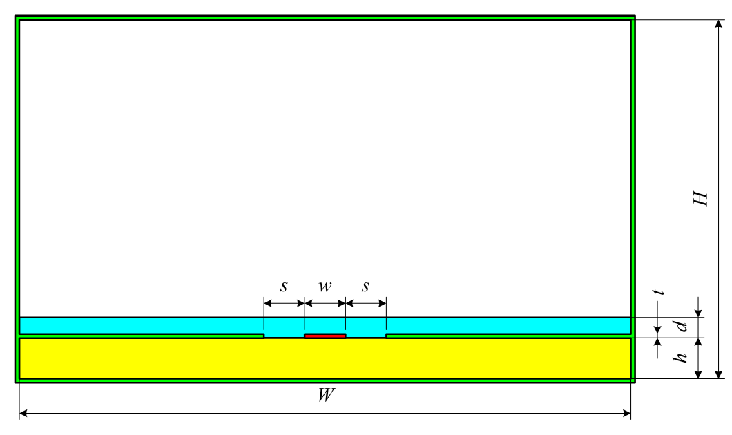
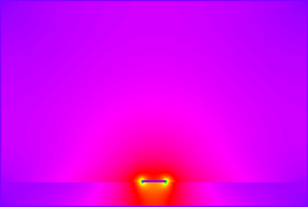
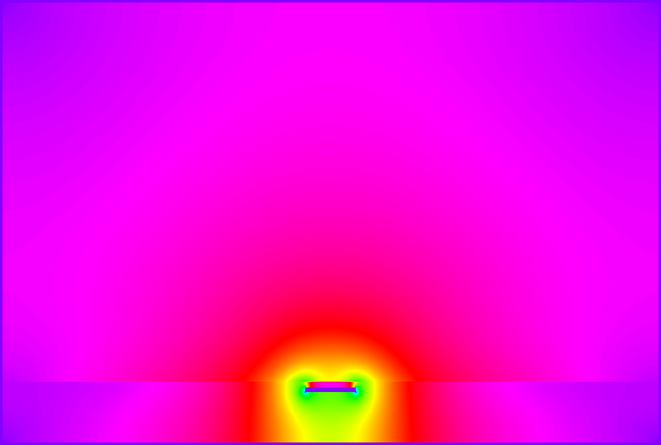
Single ended transmission lines
Simulation box configuration for the field solver
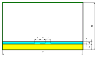
By default, H is set to 8 (h + t) and W is set to 12 h + 2 s + w; otherwise, they will be specified separately.
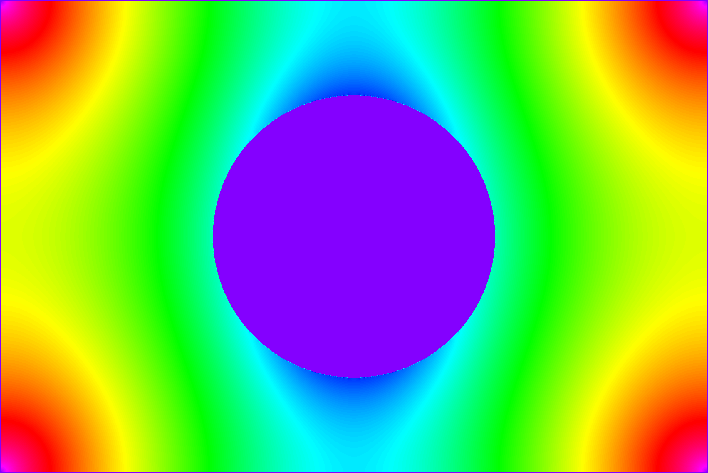
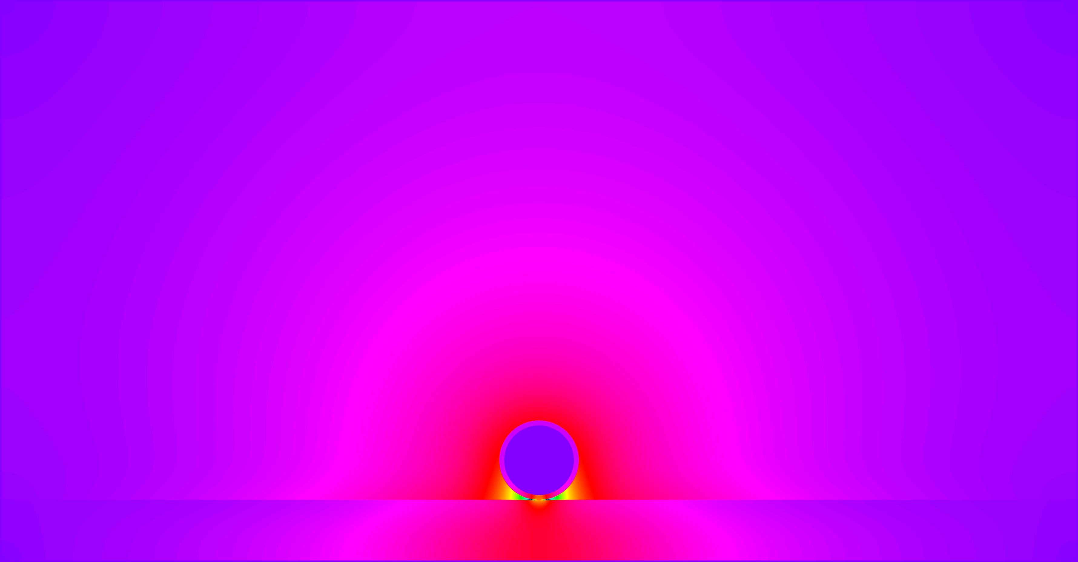
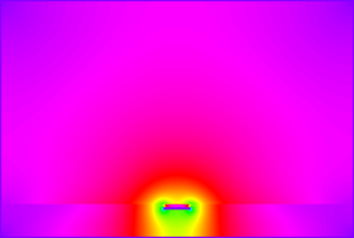
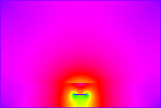
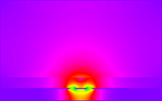
Left : Transmission line model
Right : Pseudo-color display of the absolute value of the electric field, resulting from 2D electromagnetic field solver

 Z0 ≈ 66.517 Ω
bmp4ptl -w=100 -h=100 -t=9 -strip -er=4.6 micro_stripline.bmp

 Z0 ≈ 61.927 Ω
bmp4ptl -w=100 -h=100 -t=9 -strip -er=4.6 -d=20 -ef=4.8 micro_stripline_sr.bmp

 Z0 ≈ 57.146 Ω
bmp4ptl -w=100 -h=100 -t=9 -strip -er=4.6 -d=100 -ef=4.8 micro_stripline_filler.bmp

 Z0 ≈ 43.939 Ω
bmp4ptl -w=100 -h=100 -t=9 -strip -er=4.6 -fill -H=210 stripline.bmp

 Z0 ≈ 43.442 Ω
bmp4ptl -w=100 -h=100 -t=9 -strip -er=4.6 -fill -ef=4.8 -H=210 stripline_pp.bmp

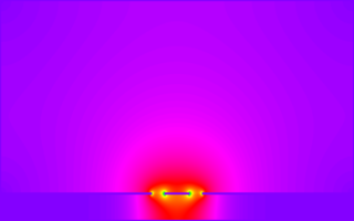 Z0 ≈ 56.095 Ω
bmp4ptl -w=100 -h=100 -t=9 -s=50 -er=4.6 conductor_backed_coplanar.bmp

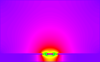 Z0 ≈ 49.420 Ω
bmp4ptl -w=100 -h=100 -t=9 -s=50 -er=4.6 -d=20 -ef=4.8 conductor_backed_coplanar_sr.bmp

 Z0 ≈ 44.285 Ω
bmp4ptl -w=100 -h=100 -t=9 -s=50 -er=4.6 -d=100 -ef=4.8 conductor_backed_coplanar_filler.bmp

 Z0 ≈ 69.575 Ω
bmp4ptl -w=50 -h=100 -t=9 -s=50 -er=4.6 -H=210 -W=350 shielded_coplanar.bmp

 Z0 ≈ 51.198 Ω
bmp4ptl -w=50 -h=100 -t=9 -s=50 -er=4.6 -fill -ef=4.8 -H=210 -W=350 channelized_coplanar.bmp
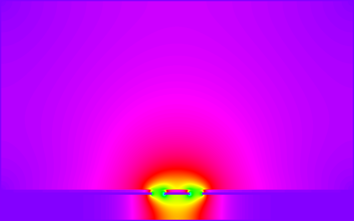
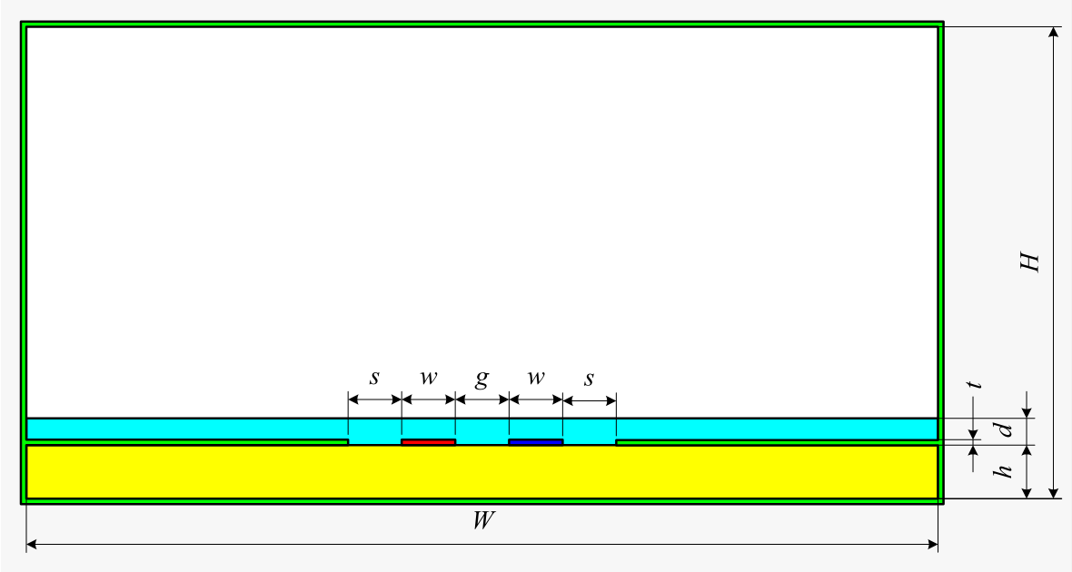
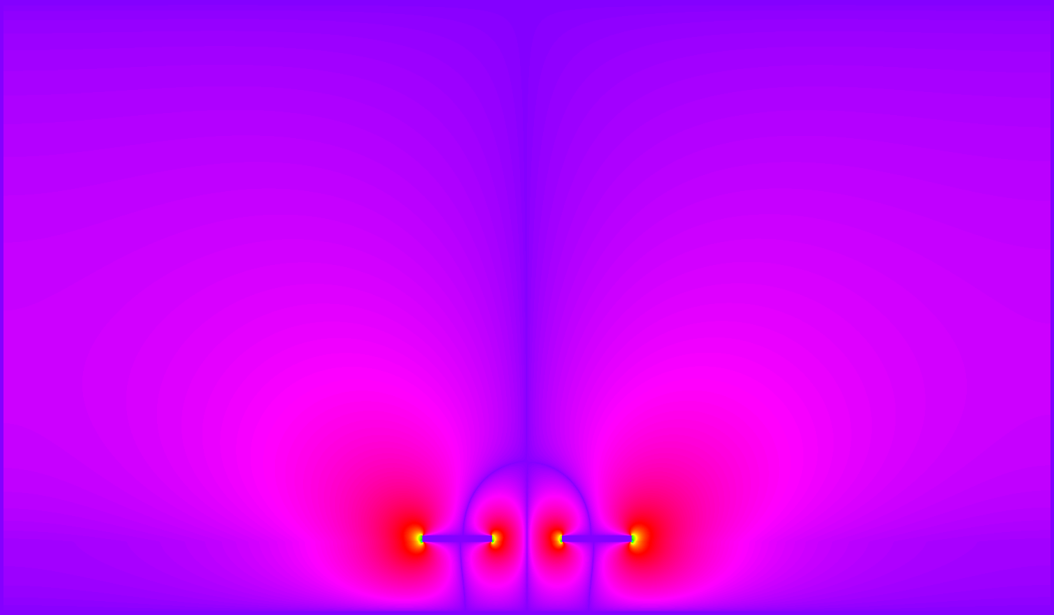
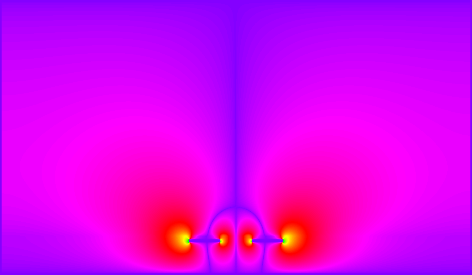
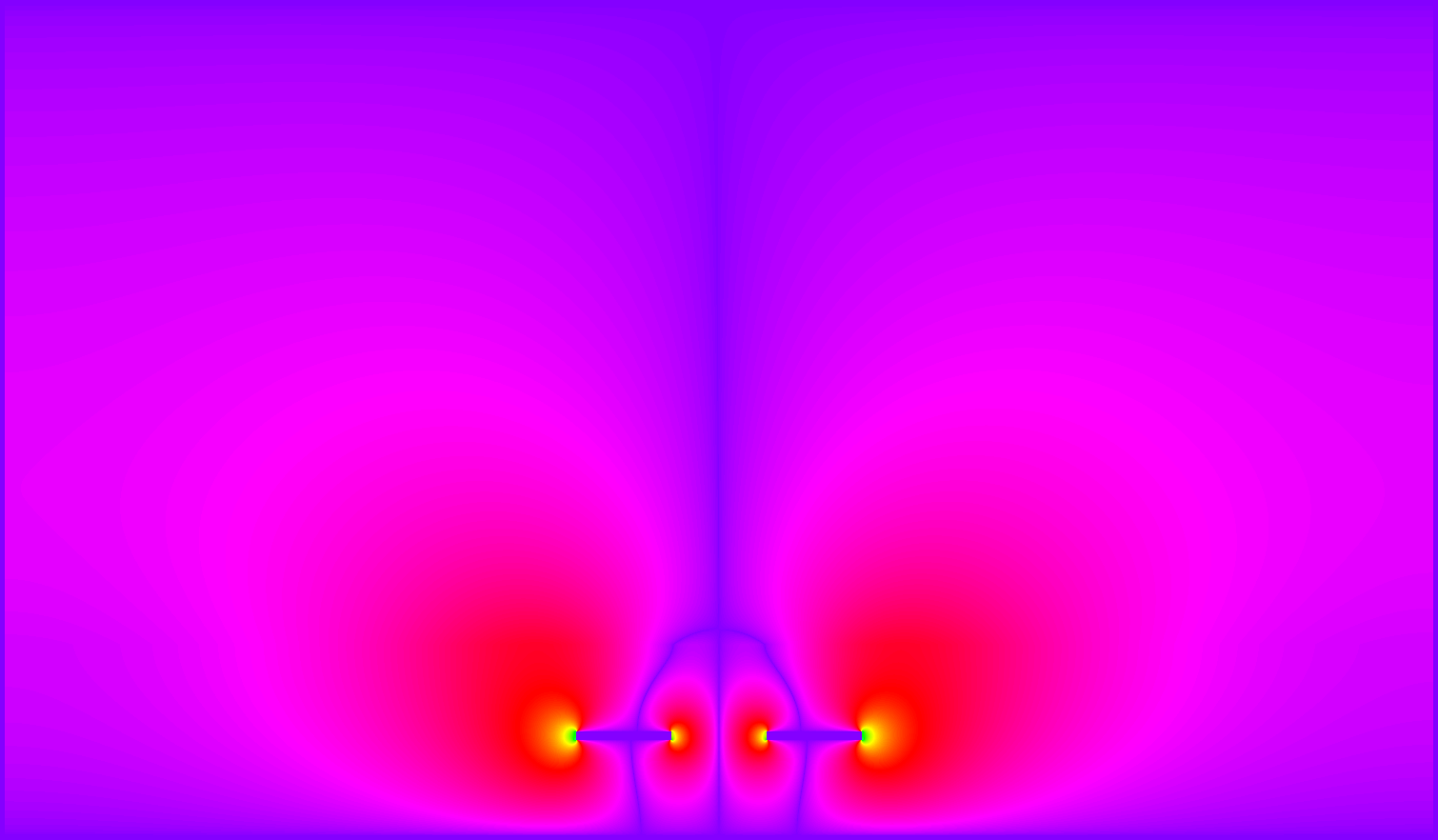
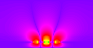
Couplers
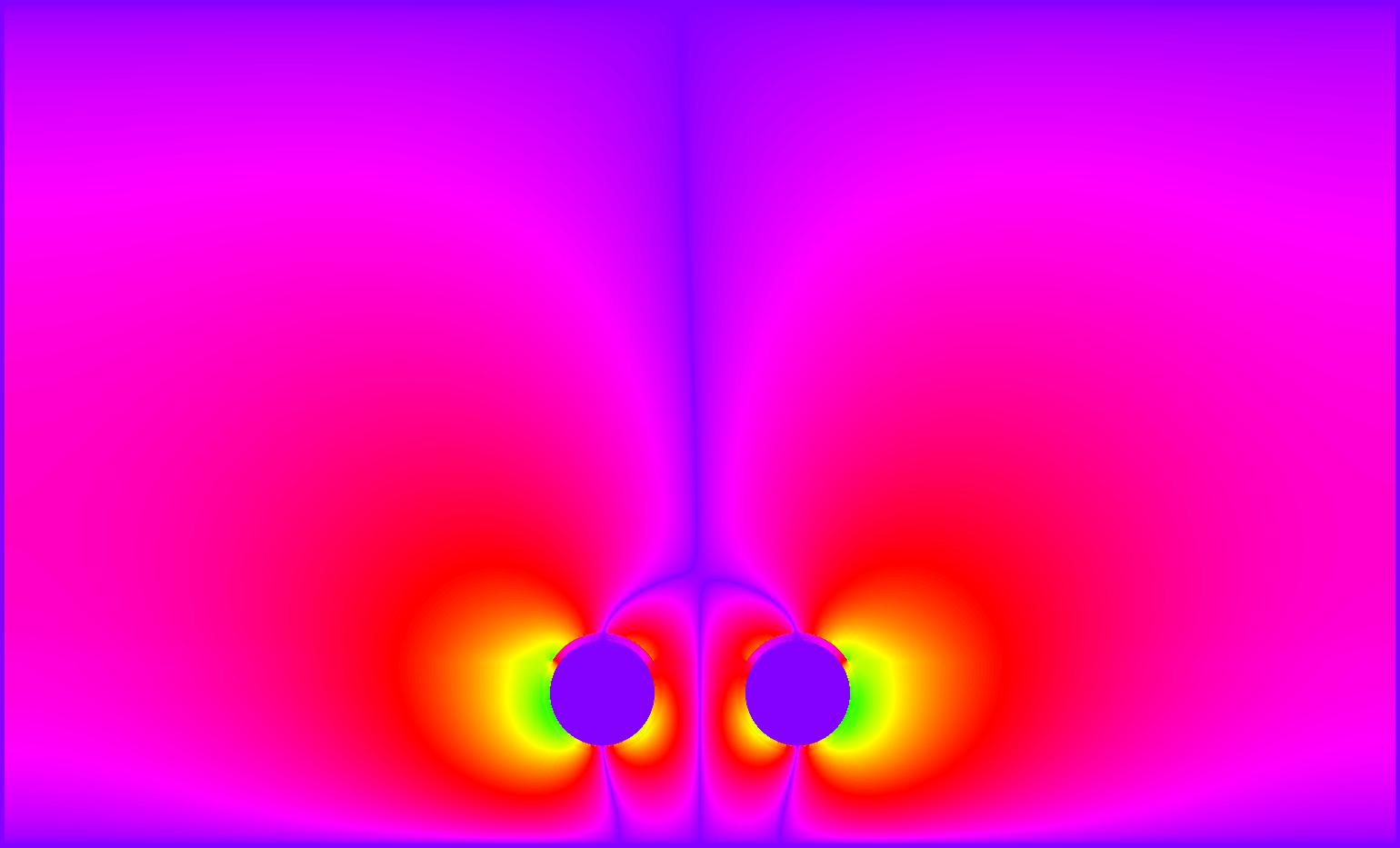
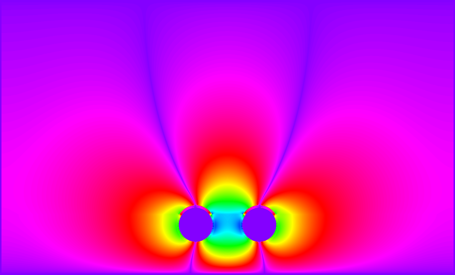
Simulation box configuration for the field solver
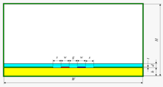
By default, H is set to 8 (h + t) and W is set to 12 h + g + 2 s + 2 w; otherwise, they will be specified separately.
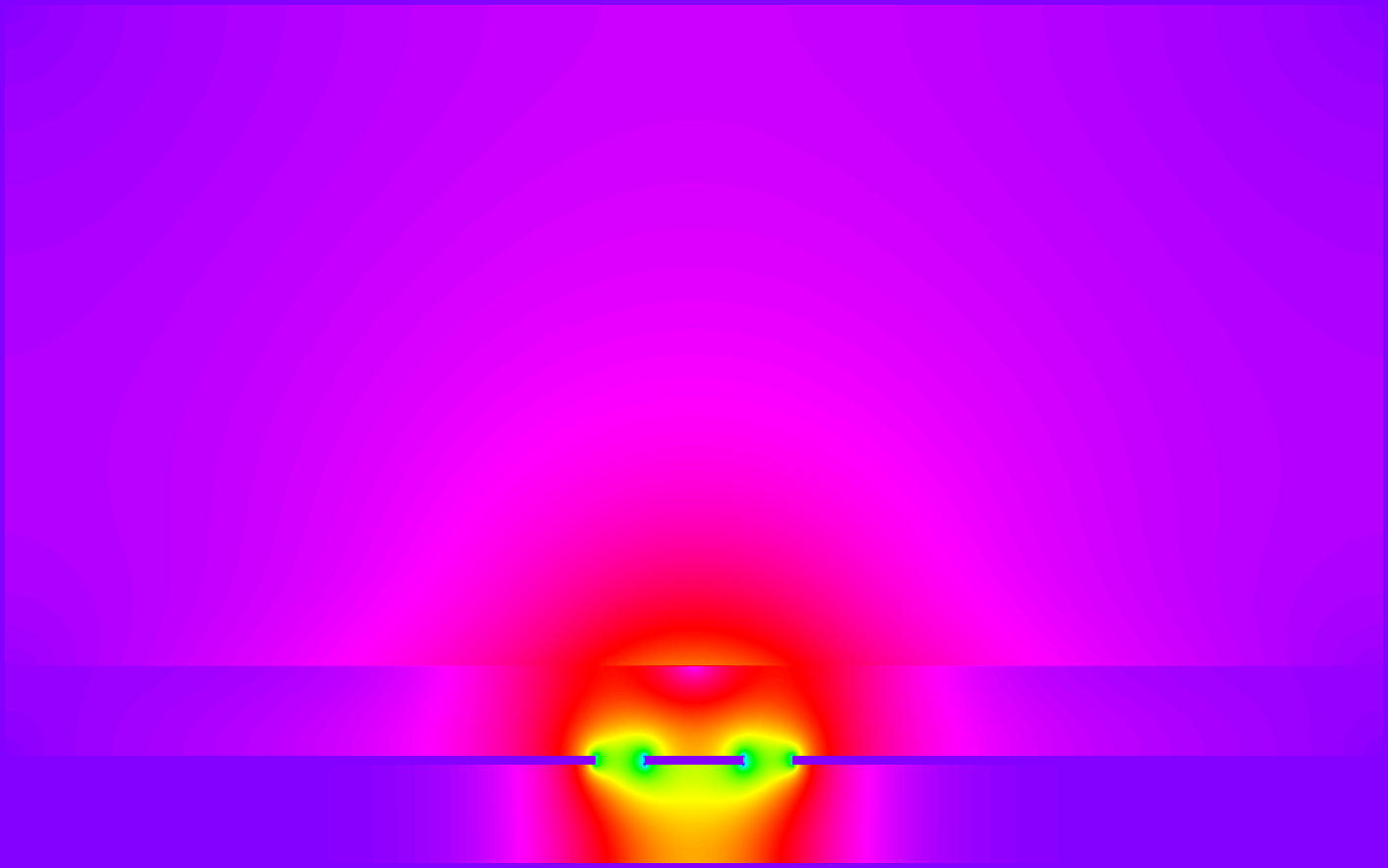
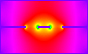
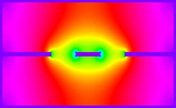
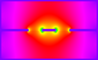
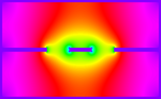
Left : Transmission line model
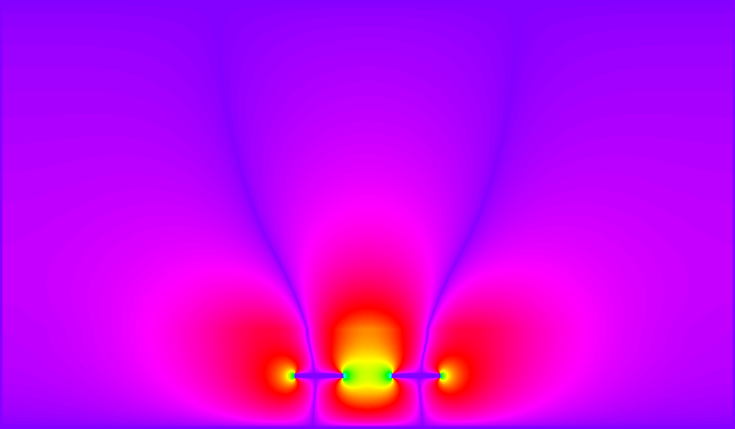
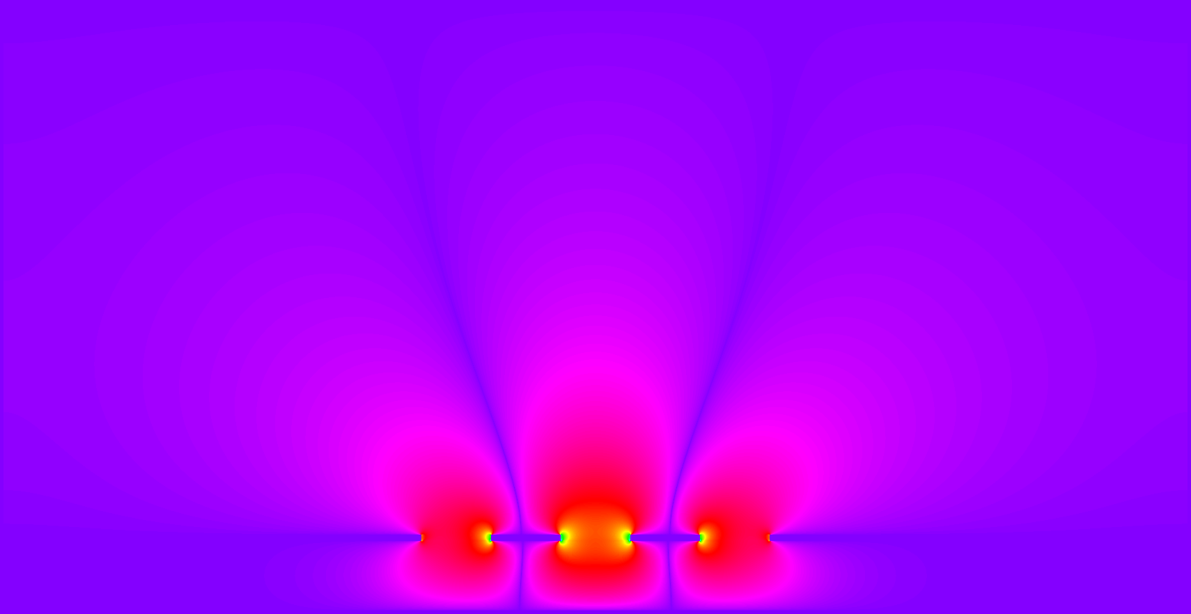
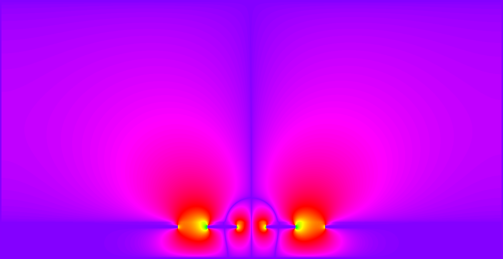
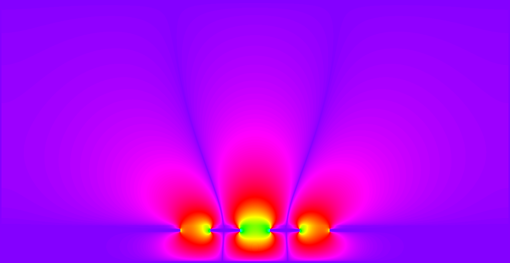
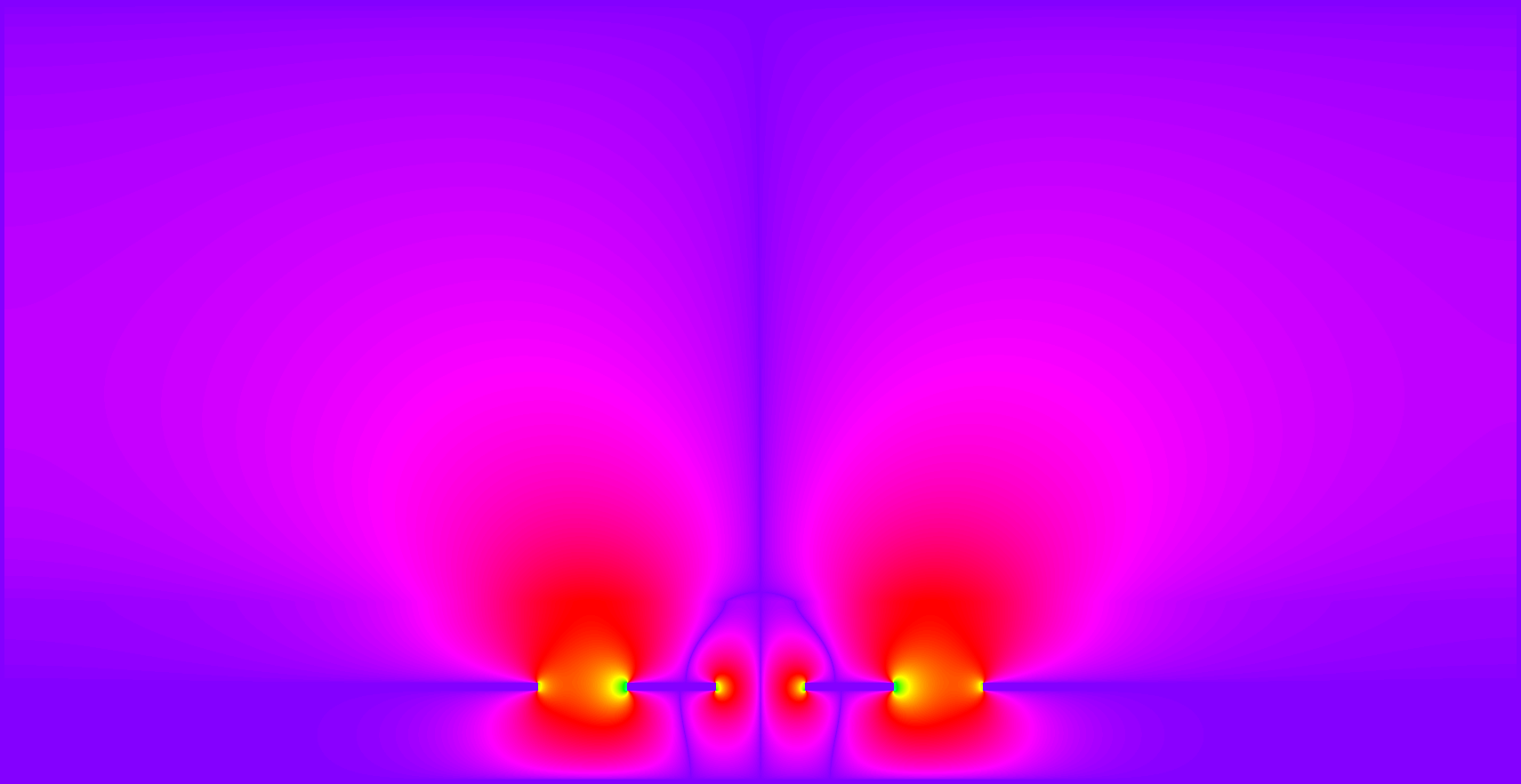
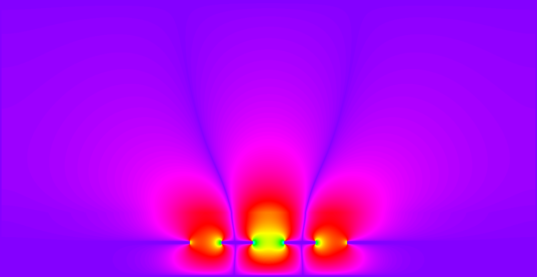
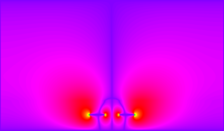
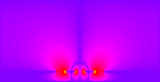
Center : Pseudo-color display of the absolute value of the electric field in even mode, resulting from 2D electromagnetic field solver
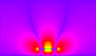
Right : Pseudo-color display of the absolute value of the electric field in odd mode, resulting from 2D electromagnetic field solver

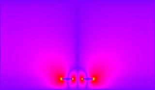
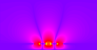
 Zeven ≈ 76.001, Zodd ≈ 56.237 Ω
bmp4ptl -w=100 -h=100 -t=9 -strip -g=100 -er=4.6 coupler_microstrip.bmp

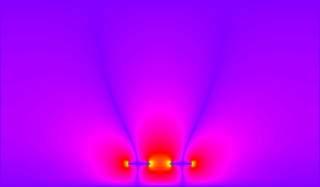
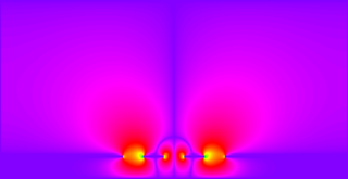
 Zeven ≈ 72.109, Zodd ≈ 50.762 Ω
bmp4ptl -w=100 -h=100 -t=9 -strip -d=20 -g=100 -er=4.6 -ef=4.8 coupler_microstrip_sr.bmp

 Zeven ≈ 68.365, Zodd ≈ 44.973 Ω
bmp4ptl -w=100 -h=100 -t=9 -strip -d=100 -g=100 -er=4.6 -ef=4.8 coupler_microstrip_filler.bmp


 Zeven ≈ 47.532, Zodd ≈ 40.000 Ω
bmp4ptl -w=100 -h=100 -t=9 -strip -g=100 -er=4.6 -fill -H=210 coupler_stripline.bmp


 Zeven ≈ 47.002, Zodd ≈ 39.540 Ω
bmp4ptl -w=100 -h=100 -t=9 -strip -g=100 -d=20 -er=4.6 -ef=4.8 coupler_microstrip_sr.bmp
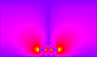
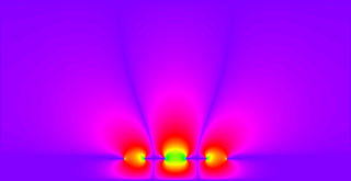
 Zeven ≈ 73.038, Zodd ≈ 55.115 Ω
bmp4ptl -w=100 -h=100 -t=9 -s=100 -g=100 -er=4.6 coupler_conductor_backed_coplanar.bmp

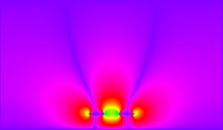
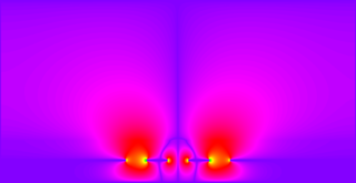
 Zeven ≈ 68.513, Zodd ≈ 49.402 Ω
bmp4ptl -w=100 -h=100 -t=9 -s=100 -g=100 -d=20 -er=4.6 -ef=4.8 coupler_conductor_backed_coplanar_sr.bmp

 Zeven ≈ 63.740, Zodd ≈ 43.462 Ω
bmp4ptl -w=100 -h=100 -t=9 -s=100 -g=100 -d=100 -er=4.6 -ef=4.8 coupler_conductor_backed_coplanar_filler.bmp
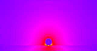
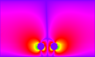
Appendix — other experimental simulations

 Z0 ≈ 42.528 Ohms Ω
bmp4ptl -w=960 -hinomaru hinomaru.bmp

 Z0 ≈ 63.406 Ohms Ω
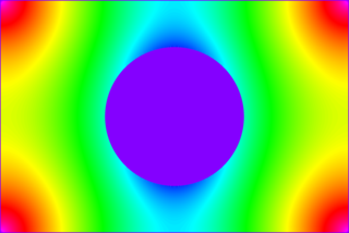
bmp4ptl -w=115 -h=100 -strip -c=8 -er=4.6 -ec=5.0 -wire wireline_enamel.bmp

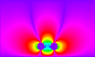 Zeven ≈ 65.743, Zodd ≈ 34.571 Ω
bmp4ptl -w=115 -h=100 -strip -c=8 -g=100 -d=100 -er=4.6 -ec=5.0 -ef=4.8 -wire coupler_wire.bmp
Download — Source code of the program used in this article
bmp4ptl-0.75.tar.gz [11 kbyte, C source code] — Creates a bitmap of cross-section of a planar transmission line.
BUGS : This program is a front-end processor for 2D field solvers, so it's not very useful by itself.
Wires with oval cross sections are not supported. Simple grids are not suitable for representing circular cross sections.
Reference
- atlc — Arbitrary Transmission Line Calculator

![[Mail]](/~lyuka/images/mail.gif)


 © 2000 Takayuki HOSODA.