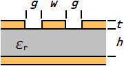
Conductor-Backed Coplanar Waveguide (CBCPW), also referred to as Grounded CPW (GCPW),
is a quasi-TEM planar transmission line consisting of a central strip conductor,
coplanar ground planes, and a backside ground plane beneath the dielectric substrate.
The present formulation is based on a quasi-static analysis employing conformal mapping techniques,
in which characteristic impedance and effective permittivity are expressed in terms of
complete elliptic integrals of the first kind.
The elliptic integral ratio is evaluated using the arithmetic-geometric mean (AGM)
to ensure numerical stability and high precision.
Classical closed-form CBCPW expressions are derived under the assumption of infinitesimally thin
(t → 0) conductors.
For practical PCB geometries, finite conductor thickness cannot be neglected.
Width-based thickness corrections are known to improve the accuracy of characteristic impedance prediction;
however, they do not necessarily preserve consistency between impedance and effective permittivity
(i.e., phase velocity).
In substrate-supported configurations,
where the electric field energy is distributed between air and dielectric regions,
this may manifest as a small but systematic deviation in the predicted effective permittivity (and thus phase constant).
In the present model, finite conductor thickness is incorporated as a first-order correction
derived from a redistribution of quasi-static field energy,
rather than by introducing an empirical capacitance term.
The correction is applied selectively to the air-side elliptic integral contribution,
with the objective of maintaining physical consistency between characteristic impedance
and effective permittivity within a unified quasi-static framework.
The correction coefficient
(α = 2.6)
has been calibrated against two-dimensional electrostatic field simulations
for representative PCB geometries.
Within validated parameter ranges,
the formulation typically agrees with two-dimensional electrostatic simulations
within a few percent for both characteristic impedance and effective permittivity.
The model is intended for engineering estimation and PCB design
in the quasi-TEM regime.
Conductor-Backed Coplanar Waveguide Analysis
CBCPW Online calculator
zcbcpw - analyze conductor-backed coplanar waveguide. Rev.1.22 (2026-03-12) (c) 2022, Takayuki HOSODA
⚠️Applicability:
See Model applicability limits in the Thickness Correction section.
η0η0 = √(μ0/ε0) = μ0c
≈ 376.730 313 412 Ω (CODATA 2022)
is the intrinsic impedance of vacuum.
K(k) denotes the complete elliptic integral of the first kind:
The argument k is the elliptic modulus.
Conductor thickness correction
The closed-form GCCPW expressions above are derived under the assumption of infinitesimally thin conductors (t → 0).
In practical PCB structures, finite conductor thickness alters the electric field distribution within the slot region.
When t > 0:
Electric field lines extend along the vertical slot sidewalls.
This primarily increases the air-side electric energy density.
The dielectric-region field distribution is only weakly perturbed under quasi-TEM conditions.
Rather than introducing an independent additional capacitance term,
the present model treats conductor thickness as a first-order redistribution of the quasi-static field energy.
Specifically, the air-side elliptic integral ratio is modified as:
where:
R1 represents the air-side elliptic integral ratio,
s is the slot width,
t is conductor thickness,
α = 2.6 is an empirically calibrated coefficient
based on 2D electrostatic field simulations for typical PCB geometries,
δ represents a first-order perturbative correction applied to the air-side elliptic ratio, reflecting the finite-thickness redistribution of the quasi-static field.
The functional form
reflects an effective sidewall field extension length associated with vertical slot surfaces,
which scales approximately with linearly t/s for thin conductors,
and gradually saturates as t becomes comparable to s.
This correction is not derived from exact conformal mapping,
but represents a physically motivated first-order modification
of the quasi-static capacitance distribution.
Within the validated parameter ranges listed below,
this thickness correction reduces the artificial sensitivity to the w/h ratio
that appears in simple linear t/s models.
By introducing a geometric saturation behavior through the
term the formulation better reflects the finite sidewall field extension.
Agreement with 2D quasi-static electrostatic simulations is typically within a few percent
for practical PCB geometries.
Model applicability limits
0.2 ≤ w/h ≤ 4.0
s/w ≤ 2.0
s/h ≤ 1.5
t/s ≤ 0.4
2.1 ≤ εr ≤ 9.8
Outside these ranges, higher-order field redistribution and non-quasi-TEM effects may introduce additional deviation.
Accuracy is primarily limited by s/h.
For s/h > 1.5,
the field distribution departs from the quasi-static conformal mapping assumption, and hybrid-mode effects increase the deviation.
When s/w becomes large,
the field configuration gradually shifts away from the canonical CPW mode toward a more weakly coupled hybrid configuration.
In these regimes, the quasi-TEM CPW formulation and the first-order thickness correction may lose accuracy.
Full-wave electromagnetic simulation is recommended once these thresholds are exceeded.
s/h exceeds approximately 1.5 or
s/w exceeds approximately 2.0.
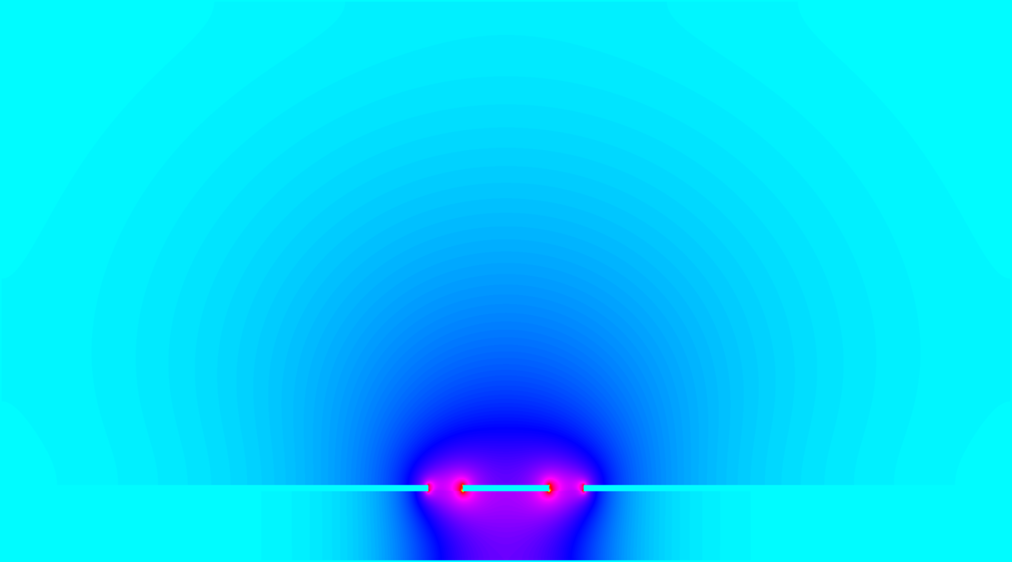
Appendix A — Electrostatic field simulation results (Examples)
Representative 2D electrostatic field simulation results used for calibration and validation of the thickness correction model.
Simulation domain dimensions:
Ground plane width W = 12h + 2s + w,
Upper boundary height H = 8(h + t).
Length unit is arbitrary.
The outer boundary is set to a ground-potential boundary condition.
w = 250, h = 200, t = 18, s = 100, εr = 4.6 → εr,eff = 2.85, Z0= 50.382 Ω w = 250, h = 200, t = 18, s = 150, εr = 4.6 → εr,eff = 2.95, Z0= 53.991 Ω w = 220, h = 200, t = 18, s = 180, εr = 4.6 → εr,eff = 2.96, Z0= 58.753 Ω
Pseudo-color map of the electric field magnitude |E| for the CBCPW structure.
w = 250, h = 200, t = 18, s = 100, εr = 4.6
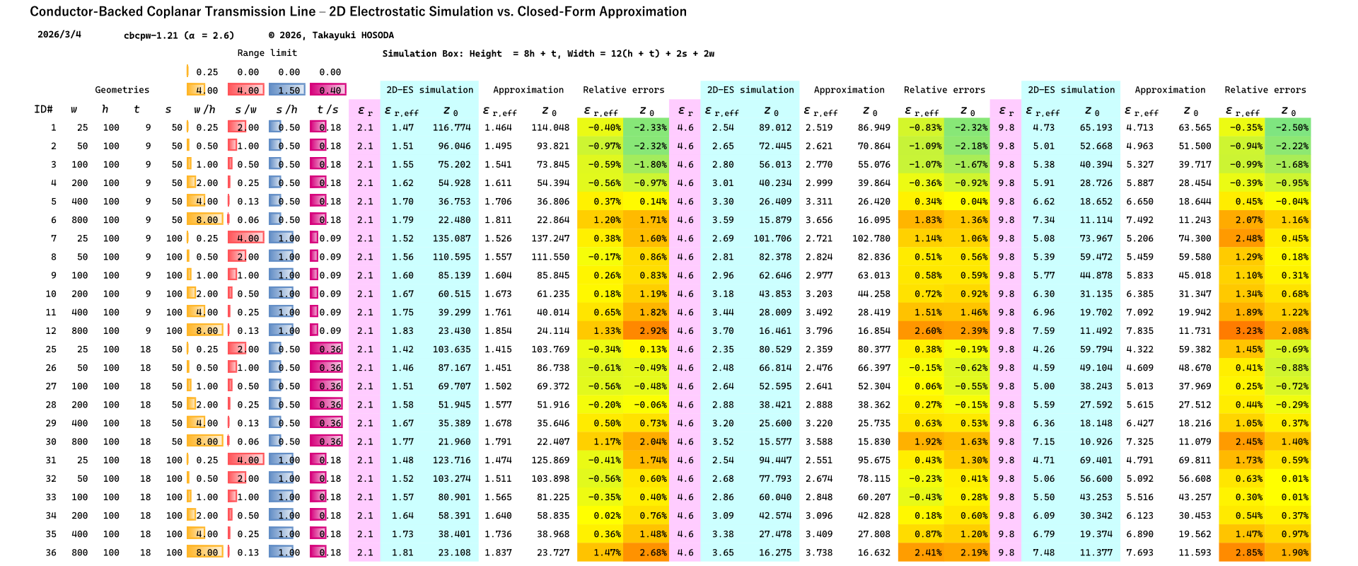
Appendix B — 2D Electrostatic Simulation vs. Closed-Form Approximation (Examples)
This appendix provides representative comparisons between the present closed-form model and
2D electrostatic field simulations for conductor-backed coplanar waveguide (CBCPW) structures.
Numerical simulation results are presented graphically for comparison only.
Tabulated raw data are intentionally omitted, since the absolute values depend on solver configuration and boundary conditions.
Within the applicability limits stated in the main text,
both effective permittivity (εr,eff) and
characteristic impedance (Z0) remain within approximately ±2.5% of the 2D electrostatic results.
For reference, when the conventional thickness correction
δ = αt / s, (α = π / 2)
is used, the deviation over the same parameter range is approximately -5.3% to +2.5% for εr,eff, and -7.2% to +1.8% for Z0.
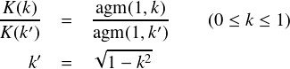
Appendix C — Relation between AGM and K(k) / K(k')
The ratio of the complete elliptic integrals of the first kind K(k) and K(k') can be calculated by the following relation with the ratio of arithmetic-geometric means (AGM).
The argument k is the elliptic modulus.
where agm(1, k) is the arithmetic-geometric mean of 1 and k.
References
R. N. Simons,
Coplanar Waveguide Circuits, Components, and Systems,
New York, NY, USA: John Wiley & Sons, 2001.
V. F. Hanna,
"Parameters of Coplanar Directional Couplers with Lower Ground Plane,"
in Proc. 15th European Microwave Conference,
1985.
W. Hilberg,
"From Approximations to Exact Relations for Characteristic Impedances,"
IEEE Transactions on Microwave Theory and Techniques,
vol. 17, no. 5, pp. 259-265, May 1969.
B. C. Wadell,
Transmission Line Design Handbook,
Norwood, MA, USA: Artech House, 1991.
G. Ghione and C. Naldi,
"Parameters of Coplanar Waveguide with Lower Ground Plane,"
Electronics Letters,
vol. 19, no. 18, pp. 734-735, Sept. 1983.
(Note: Error in equation for k1′ on p. 735.)
M. Riaziat et al.,
"Single-Mode Operation of Coplanar Waveguides,"
Electronics Letters,
vol. 23, no. 24, pp. 1281-1283, Nov. 1987.
Wentworth, Stuart M., et al.,
"The High-Frequency Characteristics of Tape Automated Bonding (TAB) Interconnects,
IEEE Transactions on Components, Hybrids, and Manufacturing Technology,
vol. 12,
no. 3,
pp. 340-347, Sept. 1989


 term the formulation better reflects the finite sidewall field extension.
Agreement with 2D quasi-static electrostatic simulations is typically within a few percent
for practical PCB geometries.
term the formulation better reflects the finite sidewall field extension.
Agreement with 2D quasi-static electrostatic simulations is typically within a few percent
for practical PCB geometries.