Synthesis and analysis
Takayuki HOSODA
Sep. 14, 2011
ustrip-3.2.js (Javascript program and Input form used in this page.)
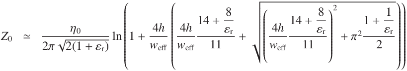
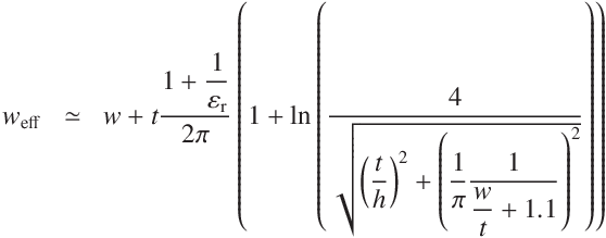
Micro strip line impedance
where,
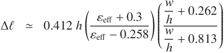
Open end effect length
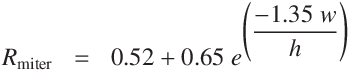
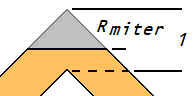
Rightangle bend compensation. Valid for w / h ≥ 0.25, ϵr ≤ 24, ± 4 % accuracy.
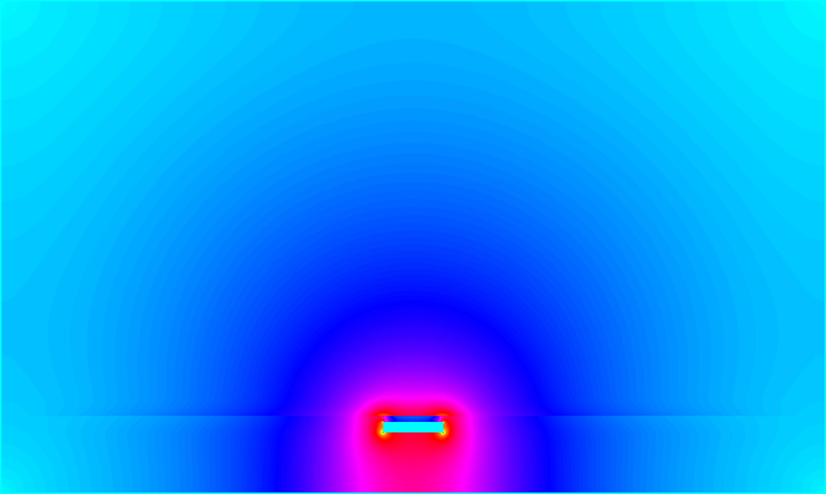
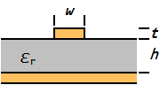
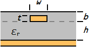
Buried microstrip line
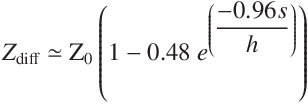
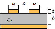
Differencial impedance of side coupled microstrip line
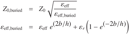
Example of field solver results (simulation box width W = 12 h + 4 t + 2 s + w, box height H = 8 h + t) Length unit in [ grid ].
w = 200, h = 200, t = 35, b = 0, ϵr=4.7, W = 2740, H = 1635 : Z0 ≃ 63.303 Ω
w = 200, h = 200, t = 35, b = 55, ϵr=4.7, W = 2740, H = 1635 : Z0 ≃ 58.388 Ω
Pseudo color visualization of absolute value of the electric field.